Advanced Microscopy
At Genuine Testing, our advanced microscopy analysis services provide unparalleled insight into the microstructure and composition of materials. Using state-of-the-art tools like Scanning Electron Microscopy (SEM), Transmission Electron Microscopy (TEM), and Dual Beam FIB/SEM, we help you uncover critical details that drive research, development, and failure analysis. Our advanced microscopy testing solutions enable you to visualize surfaces, cross-sections, and internal structures at nanoscale resolution. These methods are essential for identifying defects, analyzing coatings and films, measuring particle size, and investigating material morphology with precision.
From metals and polymers to ceramics, composites, electronic components, and nanomaterials, microscopic structure often determines macroscopic performance. Grain boundaries, porosity, inclusions, phase distribution, fiber-matrix interfaces, coating thickness, and crack propagation patterns can only be accurately evaluated through advanced imaging techniques. At Genuine Testing, we provide comprehensive advanced microscopy services using state-of-the-art instrumentation to support research and development, quality assurance, regulatory documentation, and forensic failure analysis. As an independent materials testing laboratory and Contract Research Organization (CRO), we deliver precise, defensible imaging and analytical data tailored to each application.
Why Choose Genuine Testing for Advanced Microscopy?
Comprehensive sample preparation and analysis of a wide variety of materials
Expertise in failure analysis and root cause identification
Diverse instrumentation to tackle complex challenges
Fast turnaround times and clear, actionable results
Person-to-person communication with expert staff throughout the process
Whether you’re working on process development, quality control, or troubleshooting product failures, our team is ready to support your goals with reliable data and insight.

Our Advanced Microscopy Techniques
We offer a wide array of techniques to meet your specific needs, including:
Scanning Electron Microscopy (SEM):
High-resolution imaging of surface and near-surface features with excellent depth of field. Coupled with EDS, SEM also provides elemental composition analysis.Transmission Electron Microscopy (TEM):
Ultra-high-resolution imaging of thin samples to investigate internal structures, crystallography, and elemental distribution at the atomic level.Scanning Transmission Electron Microscopy (STEM):
Combines TEM and SEM advantages for advanced failure analysis and elemental mapping.Dual Beam FIB/SEM:
Precise sample preparation and imaging, enabling “cut and look” studies of difficult-to-access features and sub-surface layers.Elemental Analysis:
Using techniques such as EDS (Energy Dispersive Spectroscopy) and EELS (Electron Energy Loss Spectroscopy) to map elemental composition and detect impurities.
Applications of Advanced Microscopy
Our advanced microscopy testing is applied to a wide range of industries and materials, including:
Nanoparticles, alloys, and metals
Thin films and coatings
Ceramics and composites
Integrated circuits and semiconductor devices
Polymers and glass substrates
We help identify:
Metal migration and voids
Cracks, delaminations, and thickness uniformity issues
Particle contamination and defect origins
Microstructural integrity of complex materials
Industries We Serve
Some of the key industries we work with include:
Electronics & Semiconductors
We help manufacturers of integrated circuits, microchips, and other semiconductor components analyze thin films, identify defects, and validate manufacturing processes with nanometer-scale accuracy.Automotive & Aerospace
Our advanced microscopy testing ensures the reliability and performance of critical materials, coatings, and assemblies in safety-critical environments, helping meet stringent industry standards.Medical Devices & Healthcare
We assist medical device developers and manufacturers in analyzing material integrity, surface coatings, and microstructure to meet regulatory requirements and ensure patient safety.Energy & Renewable Technologies
From batteries and fuel cells to solar panels and wind components, our microscopy services are used to study materials and processes that improve efficiency and longevity of energy solutions.
Optical Microscopy & Surface Examination
Optical microscopy remains a foundational tool in materials analysis. It enables rapid evaluation of surface features, grain structures, phase boundaries, inclusions, and coating layers at magnifications suitable for routine inspection and structural assessment.
Our laboratory performs brightfield, darkfield, and polarized light microscopy to examine microstructures across metals, polymers, ceramics, and composites. Metallographic preparation techniques—including sectioning, mounting, grinding, polishing, and etching—ensure clear visualization of grain boundaries and microstructural phases.
Optical microscopy supports quality control, weld inspection, coating evaluation, and initial failure assessment by providing an overview of structural integrity before higher-resolution techniques are applied.
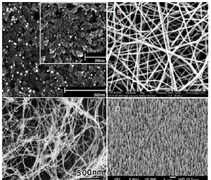
Scanning Electron Microscopy (SEM)
Scanning Electron Microscopy (SEM) provides high-resolution imaging with exceptional depth of field, allowing detailed analysis of surface topography, fracture surfaces, microcracks, porosity, and phase distribution.
Our SEM capabilities support failure analysis, coating thickness measurement, composite fiber evaluation, and microstructural characterization of advanced materials. The technique is particularly valuable for examining brittle fracture surfaces, fatigue cracks, corrosion damage, and delamination.
By combining imaging with elemental analysis capabilities, SEM enables comprehensive microstructural investigation that links structural features to material performance and degradation mechanisms.
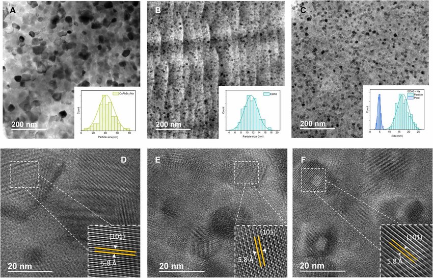
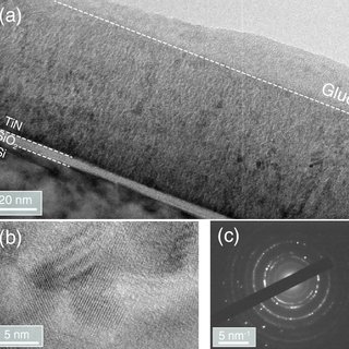
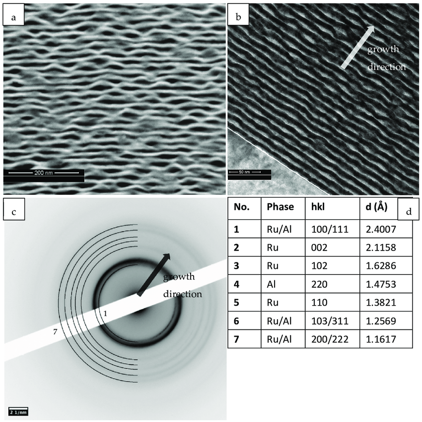
Transmission Electron Microscopy (TEM)
Transmission Electron Microscopy (TEM) allows visualization at near-atomic resolution, making it essential for nanoscale materials, thin films, and advanced functional systems.
TEM is particularly valuable in nanomaterials research, semiconductor analysis, and advanced ceramics evaluation. It provides insight into crystal structure, lattice defects, dislocations, and particle morphology at extremely high magnifications.
Our laboratory supports high-resolution imaging, selected area electron diffraction, and detailed nanostructural characterization. These analyses are critical for validating material development in cutting-edge applications such as electronics, energy storage, and nanotechnology.
Elemental Analysis & Chemical Mapping
Understanding elemental distribution is often as important as imaging structural features. Elemental analysis reveals contamination, segregation, coating composition, and phase differentiation.
We provide energy-dispersive spectroscopy (EDS) integrated with SEM to generate elemental maps and quantitative compositional data. These analyses help identify alloying elements, fillers, corrosion products, and impurity concentrations.
Chemical mapping is particularly valuable in failure investigations, coating assessments, electronic component analysis, and composite interface evaluation. By correlating microstructure with composition, we deliver deeper insight into material behavior.
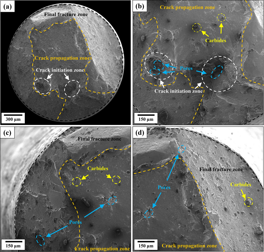
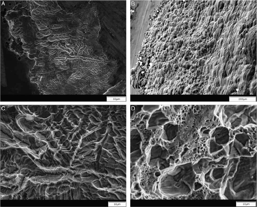
Fractography & Failure Investigation
Microscopy is central to failure analysis. Fractography—the study of fracture surfaces—reveals crack initiation points, propagation patterns, overload regions, and environmental contributions.
Our advanced microscopy services identify brittle versus ductile fracture modes, fatigue striations, corrosion-assisted cracking, and interfacial delamination. High-resolution imaging combined with compositional analysis allows precise identification of root causes.
These investigations support corrective actions, design improvements, warranty evaluations, and legal documentation. Clear visual evidence enhances reporting accuracy and technical credibility.
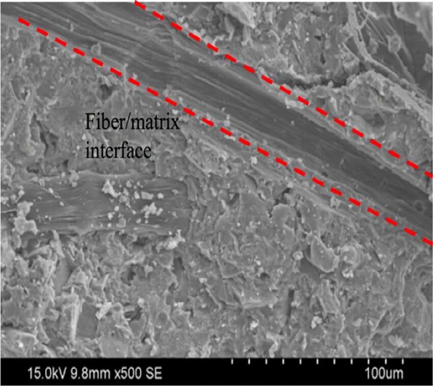
Coatings, Interfaces & Layered Systems
Layered systems—such as coatings, laminates, thin films, and composite interfaces—require precise microstructural evaluation to ensure performance integrity.
Our microscopy services assess coating thickness, adhesion quality, void presence, and interfacial bonding. Cross-sectional analysis identifies defects such as cracks, porosity, and uneven layer distribution.
For composite materials, we evaluate fiber alignment, resin distribution, and void content. In electronic materials, thin-film uniformity and interface quality are critical for electrical performance. Detailed interface analysis strengthens manufacturing control and enhances long-term durability.
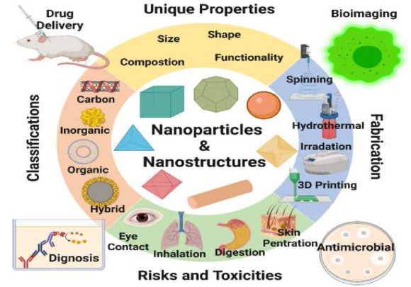
Nanomaterials & Advanced Functional Systems
Emerging materials such as nanostructured coatings, advanced composites, semiconductor films, and energy storage components demand nanoscale characterization.
Our advanced microscopy capabilities enable visualization of nanoparticle distribution, thin-film uniformity, defect density, and surface morphology at high resolution. These insights support research innovation, process optimization, and performance validation in cutting-edge technologies.
By integrating imaging with compositional analysis and mechanical testing data, we provide comprehensive characterization of advanced functional materials.
Quality Assurance & Regulatory Documentation
Advanced microscopy is essential for meeting quality assurance and regulatory documentation requirements across industries such as aerospace, automotive, electronics, medical devices, and construction.
We provide structured reporting, high-resolution imagery, quantitative measurements, and technical interpretation aligned with applicable industry standards. Independent third-party microscopy analysis strengthens supplier validation, production audits, and certification processes.
Comprehensive documentation ensures traceability, transparency, and compliance with customer and regulatory expectations.
Enabling Data-Driven Materials Innovation
Modern materials engineering increasingly depends on precise microstructural insight. Whether optimizing alloys, validating composite interfaces, characterizing electronic films, or investigating unexpected failures, advanced microscopy provides the evidence needed to guide informed decisions.
At Genuine Testing, we collaborate with engineers, manufacturers, and research teams to design customized microscopy programs tailored to specific technical challenges. Our integrated analytical approach links imaging results with mechanical, chemical, and environmental testing data to deliver a complete understanding of material behavior.
Through high-resolution imaging, elemental mapping, and expert interpretation, Genuine Testing’s advanced microscopy services empower organizations to enhance product performance, ensure quality consistency, and drive innovation with confidence.