Advanced Microscopy
At Genuine Testing, our advanced microscopy services provide deep insight into the microstructure, composition, and performance of materials across a wide range of industries. Using cutting-edge technologies including SEM analysis services, Transmission Electron Microscopy (TEM), and Dual Beam FIB/SEM systems, we help clients uncover critical information needed for research, product development, quality assurance, and forensic failure investigations. Our advanced microscopy capabilities enable detailed visualization of surfaces, interfaces, cross-sections, and internal structures at micro and nanoscale resolution. These techniques are essential for identifying defects, evaluating coatings and thin films, measuring particle morphology, and understanding material behavior with exceptional precision.
Our advanced microscopy capabilities enable detailed visualization of surfaces, interfaces, cross-sections, and internal structures at micro and nanoscale resolution. These techniques are essential for identifying defects, evaluating coatings and thin films, measuring particle morphology, and understanding material behavior with exceptional precision.
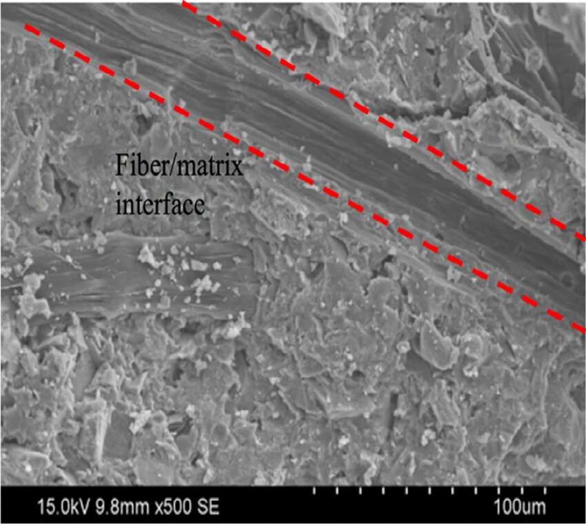
From metals and alloys to polymers, ceramics, composites, semiconductors, electronic components, and nanomaterials, microscopic structure directly impacts overall material performance. Features such as grain boundaries, porosity, inclusions, phase distribution, coating adhesion, crack propagation, and fiber-matrix bonding can only be accurately evaluated through high-resolution imaging and analytical microscopy.
As an independent materials testing laboratory and Contract Research Organization (CRO), Genuine Testing delivers accurate, defensible analytical data tailored to each application. Our advanced microscopy and scanning electron microscopy services support research institutions, manufacturers, and engineering teams with reliable results and expert technical interpretation.Why Choose Genuine Testing for Advanced Microscopy?
- Comprehensive sample preparation and analysis for a broad range of materials
- Extensive expertise in failure analysis and root cause investigation
- Advanced instrumentation for complex analytical challenges
- Fast turnaround times with detailed, actionable reporting
- Direct communication with experienced technical specialists throughout every project
Whether your focus is process development, product validation, quality control, or troubleshooting material failures, our team delivers reliable advanced microscopy solutions designed to support informed engineering decisions.

Our Advanced Microscopy Techniques
We provide a full range of advanced microscopy and SEM analysis services tailored to diverse analytical requirements.
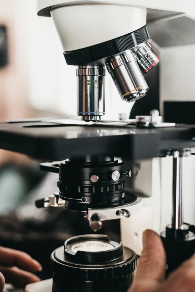
Scanning Electron Microscopy (SEM)
Our scanning electron microscopy services provide high-resolution imaging of surface and near-surface features with exceptional depth of field. SEM analysis services are widely used for evaluating fracture surfaces, porosity, corrosion damage, coatings, delamination, and microstructural features.
Transmission Electron Microscopy (TEM)
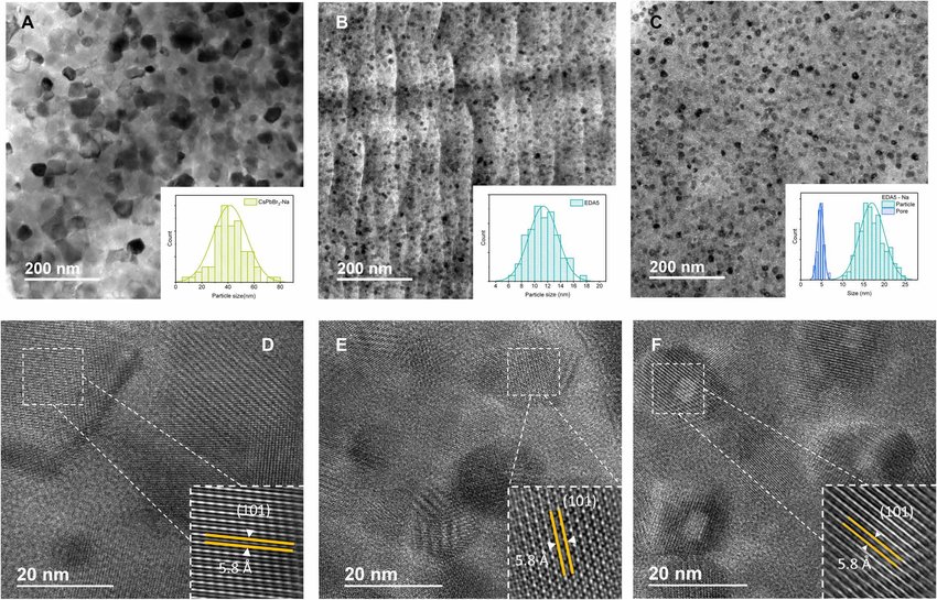
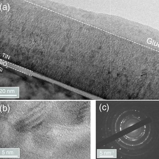
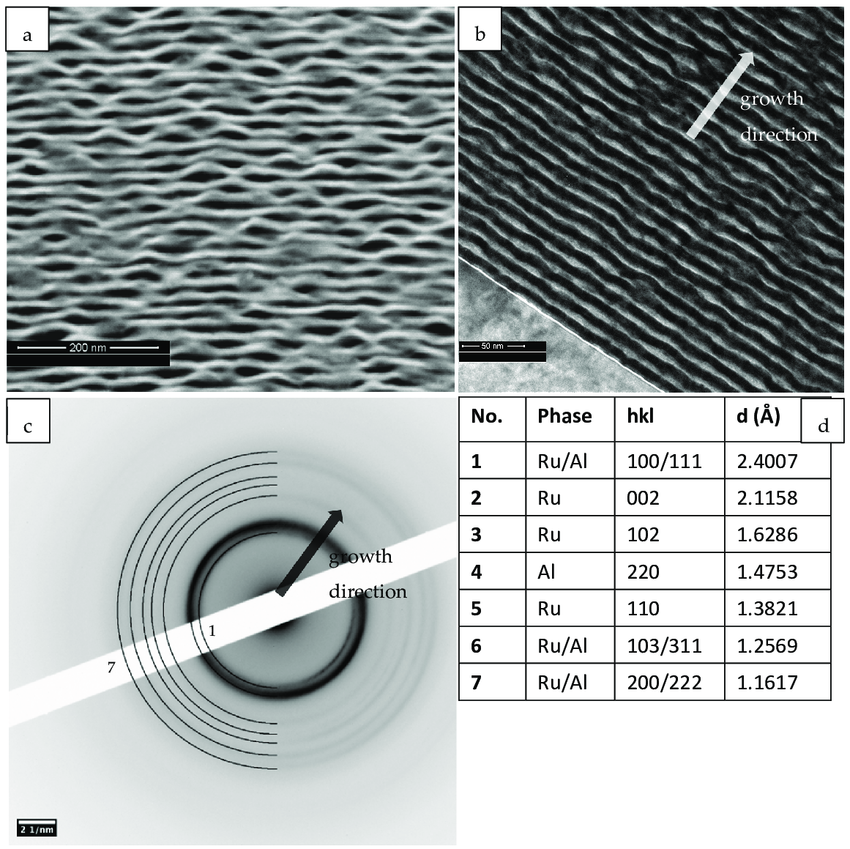
Transmission Electron Microscopy (TEM) enables ultra-high-resolution imaging of thin specimens to investigate internal structures, crystallography, lattice defects, and nanoscale morphology.
Scanning Transmission Electron Microscopy (STEM)
STEM combines the analytical advantages of SEM and TEM to provide detailed structural imaging and advanced elemental mapping capabilities. This technique is ideal for high-resolution failure analysis and nanoscale compositional investigations.
Dual Beam FIB/SEM Analysis
Dual Beam Focused Ion Beam and SEM systems enable precise “cut-and-look” investigations of subsurface structures and difficult-to-access regions. This technique supports advanced cross-sectional analysis, layered material evaluation, and semiconductor investigations.
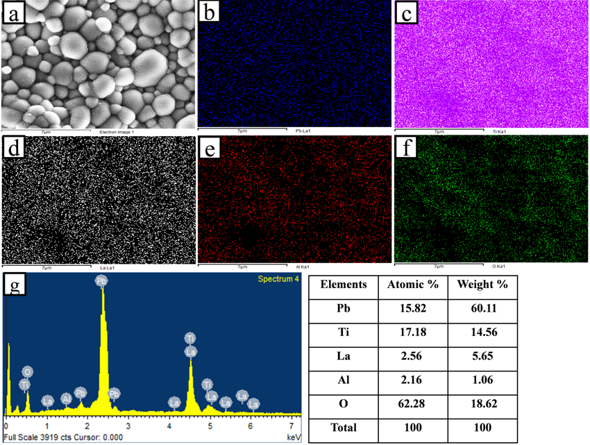
Elemental Analysis & Chemical Mapping
Understanding material composition is often as critical as structural imaging. Our advanced microscopy laboratory performs elemental mapping using EDS and Electron Energy Loss Spectroscopy (EELS) to identify impurities, compositional gradients, and phase distribution.
By correlating composition with microstructural features, we provide deeper insight into material performance and degradation mechanisms.
Applications of Advanced Microscopy
Our Advanced Microscopy and SEM analysis services support a wide range of industries and material systems, including:
- Metals and alloys
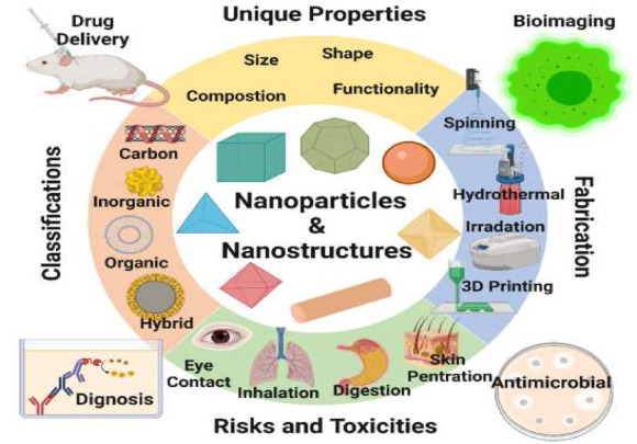
- Nanoparticles and nanostructures
- Thin films and coatings
- Ceramics and composites
- Polymers and elastomers
- Semiconductor devices
- Electronic assemblies
- Glass and optical materials
We help identify:
- Metal migration and void formation
- Surface and subsurface defects
- Cracks and delamination
- Particle contamination
- Coating inconsistencies
- Structural degradation
- Interface failures
- Thickness uniformity issues
Industries We Serve
Our advanced microscopy and scanning electron microscopy services support numerous industries, including:
- Electronics & Semiconductors
We assist manufacturers in analyzing integrated circuits, semiconductor devices, thin films, and microelectronic components with nanometer-scale precision. - Automotive & Aerospace
Our microscopy testing supports evaluation of coatings, structural materials, welds, and assemblies used in safety-critical environments. - Medical Devices & Healthcare
We help medical device manufacturers assess surface coatings, material integrity, and microstructure for regulatory compliance and product safety. - Energy & Renewable Technologies
Our analytical services support the development of batteries, fuel cells, solar materials, and renewable energy systems by characterizing material performance and degradation.
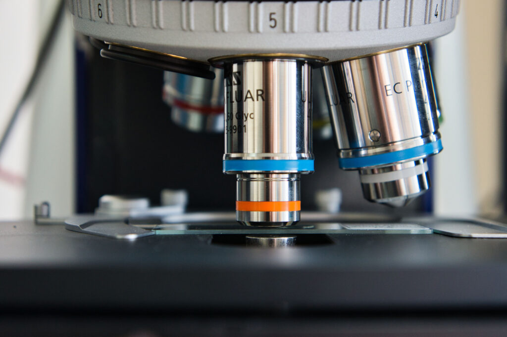
Optical Microscopy & Surface Examination
Optical microscopy remains an important component of advanced materials analysis. It enables rapid examination of grain structures, inclusions, coating layers, and surface conditions.
Our laboratory performs:
- Brightfield microscopy
- Darkfield microscopy
- Polarized light microscopy
- Metallographic preparation
- Surface morphology analysis
These methods support quality control, weld inspection, coating evaluation, and preliminary failure investigations before higher-resolution SEM analysis services are applied.
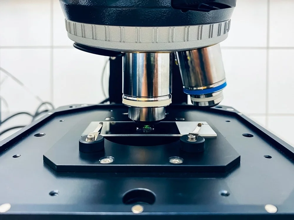
Scanning Electron Microscopy (SEM)
Scanning Electron Microscopy (SEM) provides high-resolution imaging with exceptional depth of field, allowing detailed analysis of surface topography, fracture surfaces, microcracks, porosity, and phase distribution.
Our SEM capabilities support failure analysis, coating thickness measurement, composite fiber evaluation, and microstructural characterization of advanced materials. The technique is particularly valuable for examining brittle fracture surfaces, fatigue cracks, corrosion damage, and delamination.
By combining imaging with elemental analysis capabilities, SEM enables comprehensive microstructural investigation that links structural features to material performance and degradation mechanisms.
Transmission Electron Microscopy (TEM)
Transmission Electron Microscopy (TEM) allows visualization at near-atomic resolution, making it essential for nanoscale materials, thin films, and advanced functional systems.
TEM is particularly valuable in nanomaterials research, semiconductor analysis, and advanced ceramics evaluation. It provides insight into crystal structure, lattice defects, dislocations, and particle morphology at extremely high magnifications.
Our laboratory supports high-resolution imaging, selected area electron diffraction, and detailed nanostructural characterization. These analyses are critical for validating material development in cutting-edge applications such as electronics, energy storage, and nanotechnology.
Elemental Analysis & Chemical Mapping
Understanding elemental distribution is often as important as imaging structural features. Elemental analysis reveals contamination, segregation, coating composition, and phase differentiation.
We provide energy-dispersive spectroscopy (EDS) integrated with SEM to generate elemental maps and quantitative compositional data. These analyses help identify alloying elements, fillers, corrosion products, and impurity concentrations.
Chemical mapping is particularly valuable in failure investigations, coating assessments, electronic component analysis, and composite interface evaluation. By correlating microstructure with composition, we deliver deeper insight into material behavior.
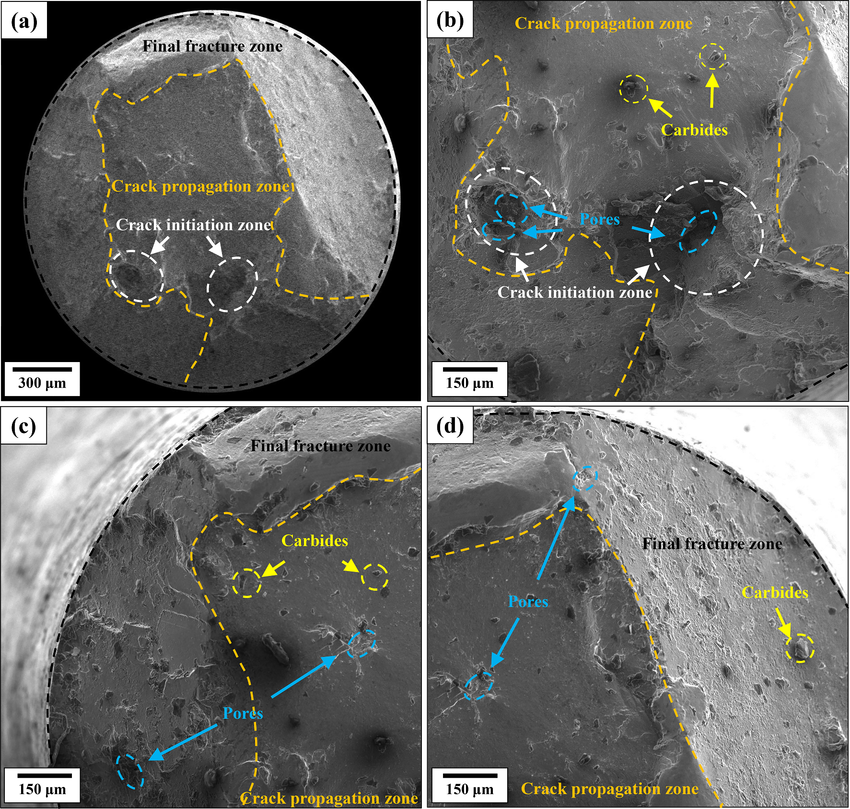
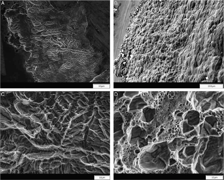
Fractography & Failure Investigation
Advanced microscopy plays a critical role in fracture and failure analysis. Through SEM analysis services and high-resolution imaging, we evaluate fracture surfaces to determine crack initiation sites, propagation patterns, overload regions, and environmental influences.
Our investigations identify:
- Brittle and ductile fracture modes
- Fatigue cracking
- Corrosion-assisted failure
- Interfacial delamination
- Stress-related damage
- Manufacturing defects
These findings support corrective action planning, design improvements, warranty claims, and technical documentation.
Coatings, Interfaces & Layered Systems
Layered systems such as coatings, laminates, thin films, and composites require precise microstructural evaluation to ensure long-term reliability.
Our scanning electron microscopy services assess:
- Coating thickness
- Adhesion quality
- Interfacial bonding
- Void distribution
- Thin-film uniformity
- Composite fiber alignment
- Resin distribution
Detailed cross-sectional analysis improves manufacturing consistency and enhances product durability.
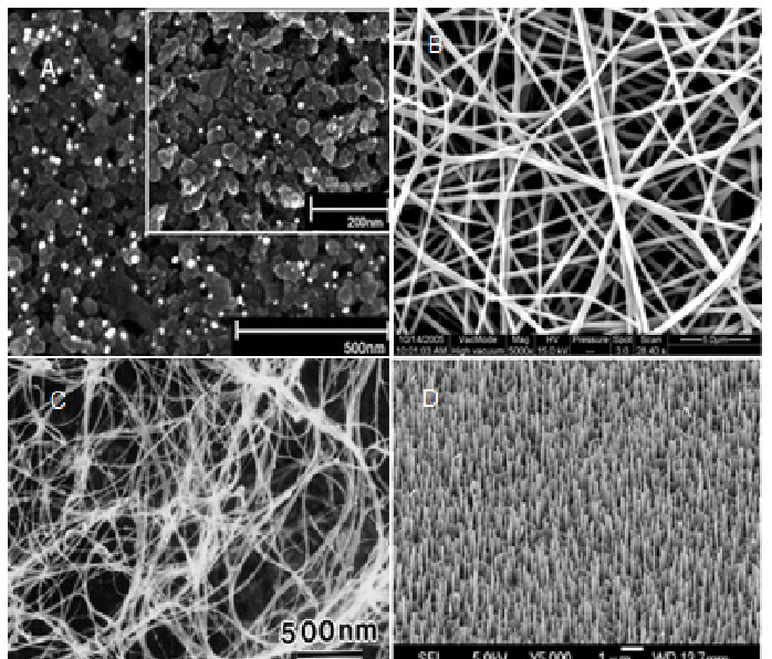
Nanomaterials & Advanced Functional Systems
Emerging technologies require advanced microscopy capable of nanoscale characterization.
Our Advanced Microscopy services support analysis of:
- Nanostructured coatings
- Semiconductor films
- Advanced composites
- Battery materials
- Energy storage systems
- Functional thin films
By integrating imaging, compositional analysis, and materials testing data, we provide comprehensive characterization of advanced functional materials.
Quality Assurance & Regulatory Documentation
Advanced microscopy and scanning electron microscopy services are essential for meeting quality assurance requirements across industries including aerospace, automotive, electronics, medical devices, and manufacturing.
We provide:
- High-resolution imaging
- Quantitative measurements
- Structured analytical reports
- Technical interpretation
- Independent third-party documentation
Comprehensive reporting ensures traceability, compliance, and confidence in product quality and material performance.
Enabling Data-Driven Materials Innovation
Modern materials engineering relies heavily on precise microstructural characterization. Whether evaluating alloys, validating coatings, analyzing semiconductor films, or investigating unexpected failures, Advanced Microscopy provides critical insight for informed engineering decisions.
At Genuine Testing, we collaborate with manufacturers, engineers, and research teams to develop customized microscopy programs tailored to complex technical challenges. By combining SEM analysis services, scanning electron microscopy services, compositional analysis, and complementary materials testing, we deliver comprehensive understanding of material behavior and performance.
Through high-resolution imaging, elemental mapping, and expert technical interpretation, our Advanced Microscopy services help organizations improve product reliability, maintain quality consistency, and accelerate innovation with confidence.
Frequently Asked Questions
We offer SEM, TEM, STEM, AFM, and optical and acoustic microscopy for high-resolution material analysis.
SEM (scanning electron microscopy) images surface details, while TEM (transmission electron microscopy) reveals internal structure at much higher magnification. Our team can recommend the right technique for your sample.
Microscopy can identify fracture patterns, contamination, microstructural defects, and corrosion that point to the root cause of failure.
Yes, all microscopy reports include annotated high-resolution images alongside written analysis.
We can accommodate a range of sample sizes; contact us with your sample dimensions to confirm compatibility.