
Semiconductor materials testing
Advanced Validation Through IPC Testing, Trace Elemental Analysis & ICP-MS Testing Services
Semiconductor and microelectronic materials form the backbone of modern digital infrastructure, supporting high-performance computing, telecommunications, automotive electronics, aerospace systems, medical technologies, and advanced consumer devices. As semiconductor architectures continue to evolve toward smaller geometries and higher processing speeds, the purity, structural integrity, and electrical stability of materials have become increasingly critical. From silicon wafers and compound semiconductors to dielectric coatings, metallization layers, and packaging interfaces, every component must satisfy demanding performance and contamination control standards.
At Genuine Testing, we provide advanced IPC Testing, Trace Elemental Analysis, and ICP-MS testing services designed to validate semiconductor and electronic material performance across manufacturing and operational lifecycles. As a specialized materials testing laboratory and Contract Research Organization (CRO), we support semiconductor manufacturers, electronics developers, integrated device manufacturers, and research organizations with accurate, defensible, and application-specific analytical data. Our multidisciplinary approach combines elemental characterization, contamination analysis, electrical validation, thermal evaluation, and advanced microscopy to ensure reliability, purity, and long-term performance consistency.
Wafer & Substrate Material Characterization
Semiconductor wafers and substrates serve as the structural and electrical foundation of microelectronic devices. Silicon remains widely used in semiconductor fabrication, while wide-bandgap materials such as gallium nitride and silicon carbide are increasingly critical for high-power and high-frequency applications. Material purity, crystallographic quality, and trace contamination levels directly affect fabrication yield and device reliability.
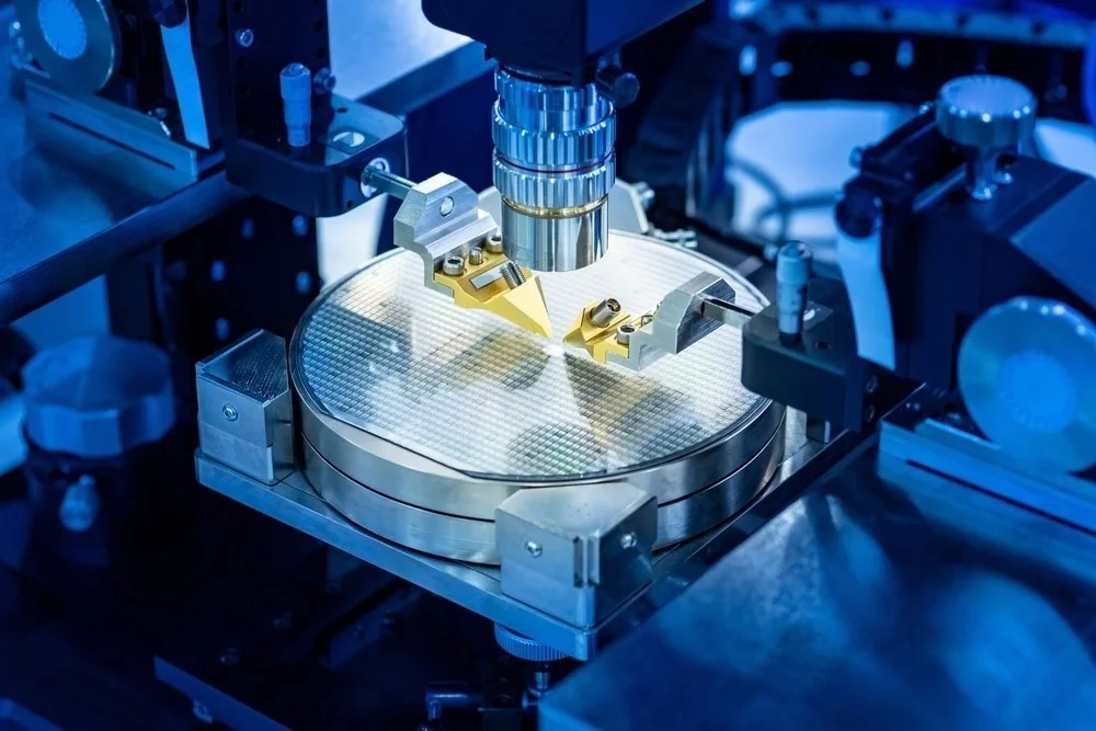
Our laboratory performs detailed wafer characterization supported by IPC Testing protocols, Trace Elemental Analysis, and ICP-MS testing services to identify metallic impurities, contamination sources, dopant inconsistencies, and microstructural defects. Advanced analytical methods evaluate crystallinity, thickness uniformity, surface integrity, and contamination levels at extremely low detection thresholds. Surface roughness and planarity assessments ensure compatibility with photolithography and thin-film deposition processes while reducing the risk of manufacturing defects.
Thin Film, Dielectric & Metallization Analysis
Modern semiconductor devices rely on multilayer thin-film structures composed of conductive, semiconductive, and insulating materials deposited at nanometer-scale thicknesses. The electrical and mechanical performance of these layers directly influences conductivity, signal integrity, and long-term reliability. Even minimal contamination or compositional variation can lead to leakage currents, resistance increases, or premature dielectric breakdown.
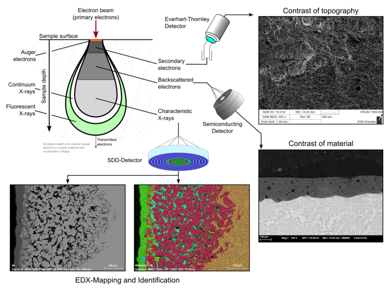
Our thin-film characterization programs incorporate IPC Testing standards alongside Trace Elemental Analysis and ICP-MS testing services to evaluate film composition, thickness uniformity, adhesion strength, grain structure, and interfacial bonding quality. Cross-sectional imaging and elemental mapping provide detailed insight into contamination distribution and defect formation within multilayer assemblies.
Dielectric materials are further evaluated for breakdown voltage, leakage current behavior, and electrical stability under operational stress conditions. Metallization layers and interconnect structures are analyzed for elemental purity, electromigration resistance, and susceptibility to stress-induced voiding, ensuring stable electrical pathways in increasingly compact device geometries.
Electrical Performance & Reliability Testing
Electrical validation is central to semiconductor materials testing. Conductivity, carrier mobility, dielectric integrity, contact resistance, and signal performance must consistently meet strict design specifications to ensure reliable device operation. Minor variations in interface quality or trace contamination can significantly impact electrical behavior and long-term stability.
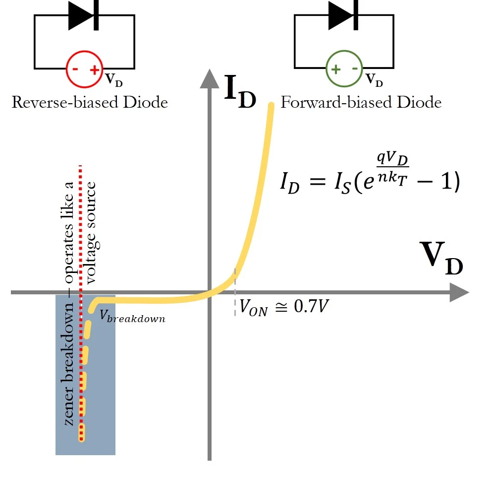
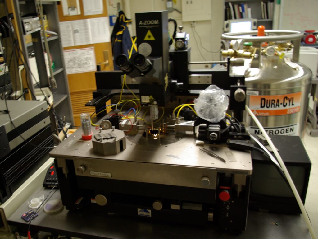
Our laboratory conducts current-voltage characterization, resistivity analysis, leakage current testing, and high-frequency electrical validation supported by IPC Testing methodologies. Trace Elemental Analysis and ICP-MS testing services help identify contamination sources that may influence conductivity, leakage behavior, or signal degradation.
Accelerated life testing and burn-in evaluations simulate extended operational conditions to identify degradation pathways and early-life failures. Electromigration studies assess the effects of sustained current flow on interconnect reliability, particularly within high-density integrated circuits. Temperature-dependent electrical testing further evaluates stability under thermal stress. By integrating elemental analysis with electrical characterization and microstructural evaluation, we provide a comprehensive understanding of semiconductor material behavior under real-world operating conditions.
Advanced Packaging & Interconnect Reliability
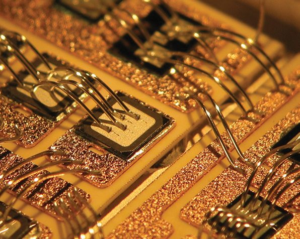
As semiconductor devices become smaller and more powerful, advanced packaging technologies play an increasingly important role in electrical connectivity, thermal management, and overall device reliability. Packaging systems involving flip-chip bonding, solder bumps, wire bonding, and multi-chip modules introduce additional material interfaces that must withstand thermal cycling, vibration, and mechanical stress.
Our testing programs evaluate solder joint integrity, bond strength, interfacial adhesion, and structural stability through advanced IPC Testing methodologies. Trace Elemental Analysis and ICP-MS testing services are used to detect contamination within solder materials, metallization layers, and packaging interfaces that could compromise electrical continuity or accelerate corrosion.
Thermal cycling evaluations simulate repeated expansion and contraction conditions that may lead to cracking, fatigue, or delamination. Shear and pull testing further assess mechanical durability and long-term interconnect reliability. Thermal conductivity analysis also supports optimization of heat dissipation within packaging assemblies, helping manufacturers reduce overheating risks and extend device lifespan.
Environmental Durability & Contamination Control
Semiconductor devices frequently operate in demanding environments involving temperature fluctuations, humidity exposure, and chemically aggressive conditions. Environmental stress can accelerate oxidation, corrosion, delamination, and electrical instability if materials are not properly validated.
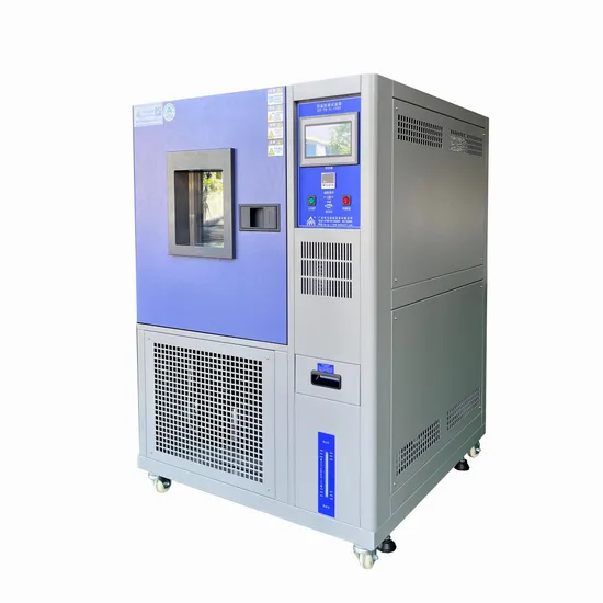
Our environmental durability programs include temperature-humidity bias testing, thermal shock analysis, and corrosion resistance evaluations aligned with IPC Testing requirements. Trace Elemental Analysis and ICP-MS testing services provide highly sensitive contamination detection capabilities that help identify trace metallic impurities, ionic contamination, and particulate residues capable of impacting fabrication yield and device performance.
Contamination control is particularly critical in cleanroom manufacturing environments, where even minimal impurity levels can significantly affect semiconductor functionality. Through detailed elemental characterization and surface analysis, we help manufacturers maintain process stability, reduce defect rates, and ensure compliance with stringent cleanliness standards.
Sub-micron imaging of semiconductor device failures — including electromigration damage, gate oxide degradation, and contact failure — is conducted through our Advanced Microscopy services using FIB-SEM cross-section preparation combined with STEM-EDS elemental analysis at the transistor level.
Failure Analysis & Root Cause Investigation
Unexpected semiconductor failures require detailed analytical investigation to identify root causes and prevent recurrence. Failures may originate from contamination, material defects, thermal overstress, process variability, or interconnect degradation. Because semiconductor devices operate at nanometer scales, advanced analytical precision is essential for accurate diagnosis.
Our failure analysis services integrate microscopy, focused ion beam cross-sectioning, electrical diagnostics, Trace Elemental Analysis, and ICP-MS testing services to identify contamination pathways, crack initiation sites, dielectric breakdown mechanisms, and metallization degradation. IPC Testing methodologies support systematic evaluation of solder integrity, assembly quality, and packaging reliability.
By combining structural, chemical, and electrical analysis, we provide actionable recommendations that support corrective actions, process optimization, improved yields, and reduced field failures.
Regulatory Compliance & Industry Standards
Semiconductor and microelectronic materials must comply with international quality, reliability, and safety standards governing automotive electronics, aerospace systems, telecommunications infrastructure, and advanced computing technologies. Qualification programs often require documented evidence of electrical performance, environmental durability, contamination control, and structural reliability.
As a specialized materials testing CRO, Genuine Testing delivers independent IPC Testing, Trace Elemental Analysis, and ICP-MS testing services aligned with industry standards and customer-specific qualification requirements. Our comprehensive reporting supports regulatory submissions, supplier audits, certification programs, and internal quality assurance initiatives. Early-stage material validation helps minimize manufacturing risk, shorten development timelines, and accelerate commercialization.
Ultra-trace metallic contamination analysis of semiconductor wafers, substrates, and process chemicals — where sub-ppb impurity levels can cause device failure — is performed through our Trace Elemental Analysis services using ICP-MS with semiconductor-grade sample preparation protocols.
Enabling Next-Generation Microelectronics
Emerging semiconductor technologies including advanced node scaling, heterogeneous integration, 3D packaging, AI hardware architectures, and wide-bandgap power devices introduce increasingly complex materials and tighter manufacturing tolerances. These advancements require highly sensitive contamination analysis and advanced validation methodologies to ensure long-term reliability.
At Genuine Testing, we collaborate with semiconductor innovators to develop customized IPC Testing, Trace Elemental Analysis, and ICP-MS testing services tailored to evolving technological demands. Our multidisciplinary expertise ensures rigorous evaluation of every material layer, interface, and package component under realistic operating conditions.
Clear, data-driven reporting empowers engineering teams to optimize designs, improve manufacturing consistency, reduce contamination-related failures, and achieve aggressive performance targets. As global demand for faster, smaller, and more energy-efficient electronics continues to expand, advanced semiconductor material validation remains essential for ensuring operational excellence and long-term device reliability.
Partner with Genuine Testing
Microelectronic materials operate under extreme conditions involving elevated temperatures, high current densities, packaging-induced mechanical stress, and environmental exposure. Even microscopic contamination or subtle compositional inconsistencies can result in signal instability, degradation, or catastrophic device failure. Through advanced IPC Testing, Trace Elemental Analysis, and ICP-MS testing services, we help manufacturers identify vulnerabilities early in development, optimize material performance, and improve high-volume manufacturing reliability.
For wide-bandgap semiconductor materials used in RF systems and power electronics, thermal conductivity, elemental purity, and electrical resistivity measurements are especially critical. By correlating elemental characterization with electrical and structural analysis, we provide comprehensive insight into substrate quality and device reliability.
Metallization layers and interconnect structures are further evaluated for contamination sensitivity, adhesion performance, electromigration resistance, and stress-induced voiding susceptibility. As semiconductor geometries continue to shrink, advanced contamination analysis and elemental characterization play an increasingly important role in maintaining stable electrical pathways and long-term microelectronic system performance.