SEM vs TEM Microscopy — What’s the Difference?
In the world of material science and industrial research, understanding the internal and surface structure of materials is essential for innovation and quality assurance. Two of the most powerful tools used for this purpose are Scanning Electron Microscopy (SEM) and Transmission Electron Microscopy (TEM).
Both fall under the umbrella of advanced microscopy, yet they serve very different purposes and deliver different types of information. Choosing between them depends on what you need to analyze—surface morphology or internal structure.
At laboratories like Genuine Testing, these techniques are part of comprehensive material evaluation services that help industries improve product reliability, performance, and compliance.
What is Scanning Electron Microscopy (SEM)?
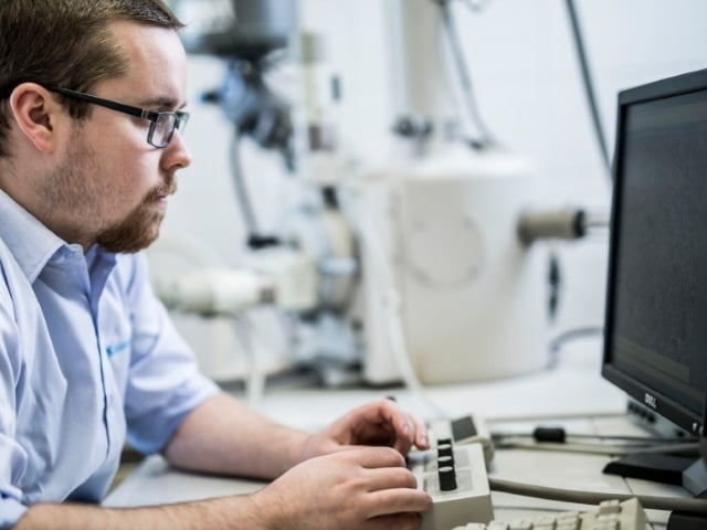
Scanning Electron Microscopy (SEM) is a technique that uses a focused beam of electrons to scan the surface of a material. When these electrons interact with the sample, they produce signals that are converted into highly detailed, three-dimensional images of the surface.
SEM is widely used in SEM analysis services because it provides:
- High-resolution surface imaging
- Depth and texture visualization
- Elemental composition analysis (with EDS integration)
- Fast and non-destructive evaluation
Key Advantages of SEM
SEM is especially valuable when surface detail matters. It allows researchers to observe cracks, corrosion, particle distribution, coating quality, and surface defects with exceptional clarity.
Industries such as aerospace, automotive, electronics, and energy rely heavily on Scanning electron microscopy to ensure materials meet strict performance standards.
What is Transmission Electron Microscopy (TEM)?
While SEM focuses on the surface, Transmission Electron Microscopy (TEM) goes deeper—literally.
In TEM, electrons are transmitted through an ultra-thin specimen. This allows scientists to study the internal structure of materials at the atomic or near-atomic level.
TEM is used to analyze:
- Internal crystal structure
- Grain boundaries
- Defects at atomic scale
- Nano-scale particles and structures
Key Advantages of TEM
TEM offers much higher magnification and resolution than SEM, making it ideal for nanotechnology, advanced materials research, and semiconductor development. However, sample preparation is more complex, requiring ultra-thin sections.
SEM vs TEM — Key Differences
Although both techniques are essential in Advanced microscopy, they differ significantly in function, capability, and application.
1. Imaging Focus
- SEM: Surface structure and morphology
- TEM: Internal structure and atomic-level details
2. Magnification & Resolution
- SEM: High resolution (up to nanometer scale)
- TEM: Extremely high resolution (atomic scale possible)
3. Sample Preparation
- SEM: Minimal preparation, relatively simple
- TEM: Complex preparation, ultra-thin samples required
4. Type of Information
- SEM: 3D-like surface images and composition
- TEM: 2D projection of internal structure
5. Applications
- SEM: Material failure analysis, surface coating inspection, contamination detection
- TEM: Nanotechnology research, crystal structure analysis, semiconductor studies
Understanding these differences helps researchers and engineers choose the right tool for precise material characterization.
Applications of Advanced Microscopy in Industry
Both SEM and TEM play a vital role in modern industrial research and product development. Through advanced microscopy, companies can detect material defects early, improve quality control, and accelerate innovation.
Common Applications Include:
- Failure analysis of mechanical components
- Quality inspection of coatings and surfaces
- Semiconductor and microchip analysis
- Battery material research
- Polymer and composite evaluation
- Nanomaterial development
Industries such as healthcare, energy, construction, and electronics depend on microscopy data to ensure safety, compliance, and performance.
Why SEM Analysis Services Matter in Modern Research
Today’s industries demand precision. Even microscopic defects can lead to major product failures. This is where professional SEM analysis services become critical.
By using scanning electron microscopy, laboratories can provide:
- Accurate defect identification
- Surface contamination detection
- Material comparison and validation
- High-resolution imaging for R&D support
At Genuine Testing, SEM services are integrated into a broader Contract Research Organization (CRO) framework. This ensures clients not only receive data but also actionable scientific insights that support decision-making.
Advanced Microscopy for Innovation and Compliance
Modern product development is driven by science, and advanced microscopy is at the heart of that innovation. Whether it’s improving the durability of aerospace components or enhancing battery efficiency, SEM and TEM together provide a complete picture of material behavior.
With the right laboratory partner, businesses can move from hypothesis to commercialization faster, with confidence in every material decision.
Conclusion
While SEM (Scanning Electron Microscopy) and TEM (Transmission Electron Microscopy) are both powerful imaging techniques, they serve different purposes in material science. SEM is ideal for surface analysis and structural visualization, while TEM provides deep insights into internal atomic structures.
Together, they form the backbone of advanced microscopy, enabling industries to innovate, improve quality, and maintain compliance.
With expert-driven SEM analysis services and comprehensive laboratory capabilities, organizations like Genuine Testing empower industries to transform complex scientific challenges into reliable, real-world solutions.